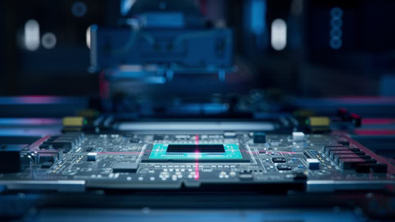
Precision Silicon. Global Innovation.
We turn complex design into smarter solutions
A process where intricate engineering challenges are simplified into intelligent, functional products for the global market.
Read more
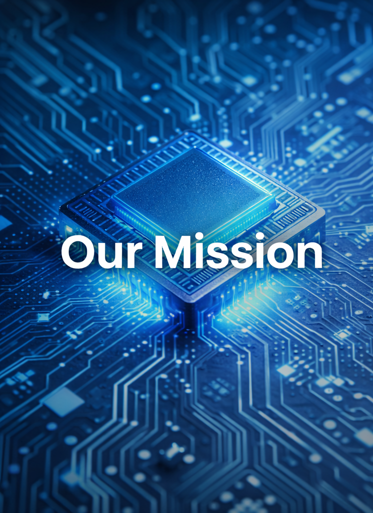
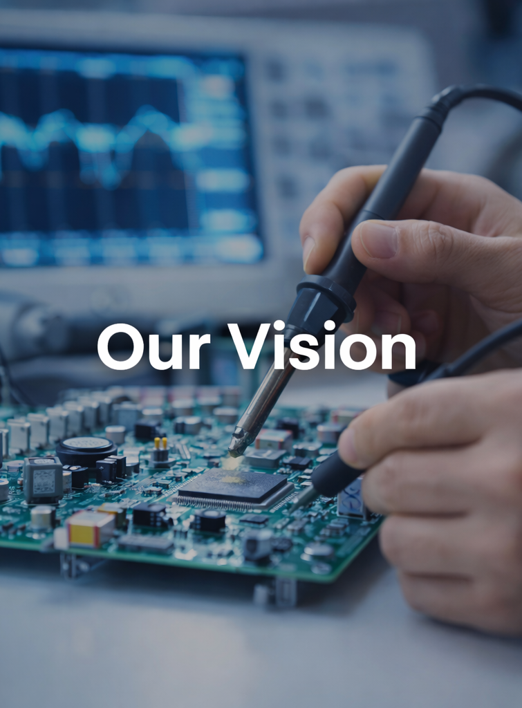
Innovating Semiconductor,
OSAT Design.
Delivering cutting-edge Semiconductor,OSAT,Embedded and PCB design services for next-generation electronics.
Continue Reading